
전력 MOSFET smd 110v STC2326
최신 가격을 얻으십시오| 지불 유형: | L/C,T/T,Paypal |
| 인 코텀: | FOB,CFR,CIF |
| 수송: | Ocean,Air |
| 포트: | SHANGHAI |

모형: YZPST-STC2326
상표: YZPST
B TA30 시리즈 트라이 액
YZPST-STC2326
기술
STC2326은 초고밀 셀 밀도 DMOS 트렌치 기술을 사용하여 만들어진 N- 채널 로직 향상 모드 전력 필드 효과 트랜지스터이다. STC2326은 동기 또는 기존 스위칭 PWM 컨트롤러를 사용하여 DC / DC 컨버터의 전체 효율을 향상 시키도록 특별히 설계되었다. 낮은 게이트 전하, 낮은 RDS (ON) 및 빠른 스위칭 속도를 위해 최적화되었습니다.
응용 프로그램
전원 시스템
DC / DC 컨버터
로드 스위치
풍모
110V / 3A, RDS (ON) = 310mΩ @ VGS = 10V
매우 낮은 RDS (ON)을위한 고밀도 셀 설계
탁월한 온 저항 및 최대 DC 전류 성능
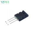
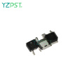
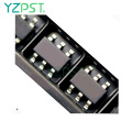
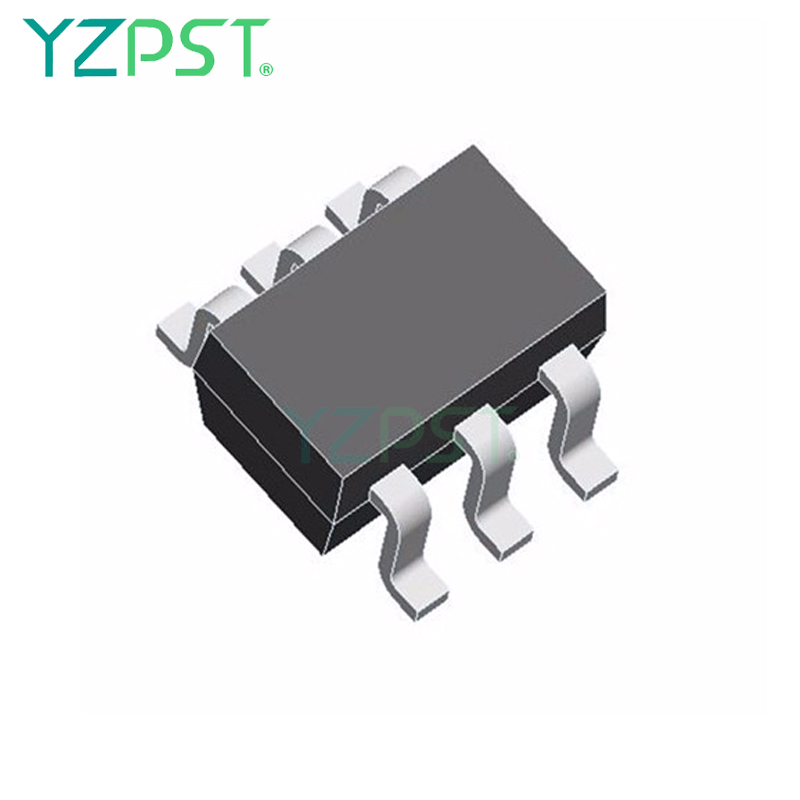
SOT-23-6L 패키지 디자인
핀 구성 (SOT-23-6L)
")
|
Pin |
Symbol |
Description |
|
1 |
D |
Drain |
|
2 |
D |
Drain |
|
3 |
G |
Gate |
|
4 |
S |
Source |
|
5 |
D |
Drain |
|
6 |
D |
Drain |
O RDER ING F O R은 T M N O I IN
|
Part Number |
Package |
Part Marking |
|
SPN2326S26RGB |
SOT-23-6L |
26YW |
A B SOU L T E MA X I M U M R A T IN G S ( T A = 25 ℃ U n l e s s O t H E R w I S E n o t e d )
|
Parameter |
Symbol |
Typical |
Unit |
|
|
Drain-Source Voltage |
VDSS |
110 |
V |
|
|
Gate –Source Voltage |
VGSS |
±20 |
V |
|
|
Continuous Drain Current(TJ=150℃) |
TA=25℃ |
ID |
3.0 |
A |
|
TA=70℃ |
2.0 |
|||
|
Pulsed Drain Current |
IDM |
10 |
A |
|
|
Power Dissipation |
TA=25℃ |
PD |
2.0 |
W |
|
TA=70℃ |
1.3 |
|||
|
Operating Junction Temperature |
TJ |
-55/150 |
℃ |
|
|
Storage Temperature Range |
TSTG |
-55/150 |
℃ |
|
|
Thermal Resistance-Junction to Ambient |
RθJA |
62.5 |
℃/W |
|
|
Parameter |
Symbol |
Conditions |
Min. |
Typ |
Max. |
Unit |
|
Static |
||||||
|
Drain-Source Breakdown Voltage |
V(BR)DSS |
VGS=0V,ID=250uA |
110 |
|
|
V |
|
Gate Threshold Voltage |
VGS(th) |
VDS=VGS,ID=250uA |
1 |
2.0 |
2.5 |
|
|
Gate Leakage Current |
IGSS |
VDS=0V,VGS=±20V |
|
|
±100 |
nA |
|
Zero Gate Voltage Drain Current |
IDSS |
VDS=80V,VGS=0V |
|
|
1 |
uA |
|
VDS=80V,VGS=0V TJ=125℃ |
|
|
5 |
|||
|
On-State Drain Current |
ID(on) |
VDS≥5V,VGS =10V |
3.0 |
|
|
A |
|
Drain-Source On-Resistance |
RDS(on) |
VGS= 10V,ID=3A |
|
0.26 |
0.31 |
Ω |
|
Forward Transconductance |
gfs |
VDS=10V,ID=3A |
|
2.4 |
|
S |
|
Diode Forward Voltage |
VSD |
IS=1A,VGS =0V |
|
|
1.2 |
V |
|
Dynamic |
||||||
|
Total Gate Charge |
Qg |
VDS=80V,VGS=10V ID= 5A |
|
9 |
13 |
nC |
|
Gate-Source Charge |
Qgs |
|
2 |
|
||
|
Gate-Drain Charge |
Qgd |
|
1.4 |
|
||
|
Input Capacitance |
Ciss |
VDS=25,VGS=0V f=1MHz |
|
508 |
|
pF |
|
Output Capacitance |
Coss |
|
29 |
|
||
|
Reverse Transfer Capacitance |
Crss |
|
16.5 |
|
||
|
Turn-On Time |
td(on) |
VDD=50V,RL=10Ω ID=3A,VGEN=10V RG=3.3Ω |
|
2 |
|
nS |
|
tr |
|
21.5 |
|
|||
|
Turn-Off Time |
td(off) |
|
11.2 |
|
||
|
tf |
|
18.8 |
|
|||
")
")


전화 번호: 86-514-87782298
Whatsapp: +8613805278321
회사 주소: 3rd Floor, Weiheng Building No.20 B Area, Yangzhou, Jiangsu China
웹 사이트: https://kr.yzpst.com


Privacy statement: Your privacy is very important to Us. Our company promises not to disclose your personal information to any external company with out your explicit permission.
Fill in more information so that we can get in touch with you faster
Privacy statement: Your privacy is very important to Us. Our company promises not to disclose your personal information to any external company with out your explicit permission.