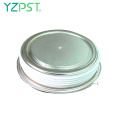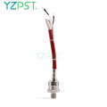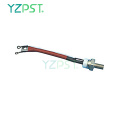

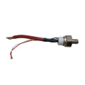

높은 DV/DT 기능 320A 위상 제어 사이리스터
$452-49 Piece/Pieces
$39≥50Piece/Pieces
| 지불 유형: | L/C,T/T,Paypal |
| 인 코텀: | FOB,CFR,CIF |
| 수송: | Ocean,Air |
| 포트: | Shanghai |

$452-49 Piece/Pieces
$39≥50Piece/Pieces
| 지불 유형: | L/C,T/T,Paypal |
| 인 코텀: | FOB,CFR,CIF |
| 수송: | Ocean,Air |
| 포트: | Shanghai |
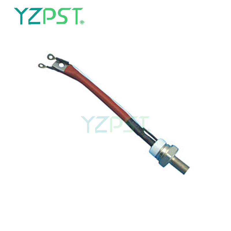
모형: YZPST-T171-320-10
상표: yzpst
공급 유형: 원래 제조업체
참고 자료: 사진, 다른
구성: 정렬
현재 분석: 해당 없음
작동 온도: -40 ° C ~ 125 ° C
SCR 유형: 민감한 게이트
구조: 단일
전압 켜기: 해당 없음
전압 게이트 트리거 (Vgt) (최대): 해당 없음
전류 출력 (최대): 해당 없음
ITRMS: 502A
ITSM: 7kA
IH: 300mA
| 판매 단위 | : | Piece/Pieces |
| 다운로드 | : |
|

위상 제어 사이리스터
YZPST-T171-320-10
특징
중앙 증폭 게이트 구성
압축 결합 캡슐화
높은 DV/DT 기능
스터드 유형, 나사산 인치 또는 메트릭
일반적인 응용 프로그램
중간 전원 스위칭
DC 전원 공급 장치
최대 등급 및 특성
|
Symbol |
Parameter |
Values |
Units |
Test Conditions |
|
|
ON-STATE |
|
|
|
||
|
ITAV |
Mean on-state current |
320 |
A |
Sinewave,180° conduction,Tc=84oC |
|
|
ITRMS |
RMS value of on-state current |
502 |
A |
Nominal value |
|
|
ITSM |
Peak one cycle surge (non repetitive) current |
7 |
kA |
10.0 msec (50Hz), sinusoidal wave- shape, 180o conduction, Tj = 125 oC |
|
|
I2t |
I square t |
240 |
KA2s |
8.3 msec and 10.0 msec |
|
|
IL |
Latching current |
700 |
mA |
VD = 24 V; RL= 12 ohms |
|
|
IH |
Holding current |
300 |
mA |
VD = 24 V; I = 2.5 A |
|
|
VTM |
Peak on-state voltage |
1.6 |
V |
ITM = 1005 A |
|
|
di/dt |
Critical rate of rise of on-state current |
non-repetitive |
1000 |
A/ms |
Gate drive 20V, 20Ω, tr≤1μs, Tj=Tjmax, anode voltage≤80% VDRM |
|
repetitive |
- |
||||
|
BLOCKING |
|
|
|
||
|
VDRM VRRM |
Repetitive peak off state voltage Repetitive peak reverse voltage |
1000 |
V |
|
|
|
VDSM VRSM |
Non repetitive peak off state voltage Non repetitive peak reverse voltage |
1100 |
V |
|
|
|
IDRM IRRM |
Repetitive peak off state current Repetitive peak reverse current |
70 |
mA |
Tj = 100 oC ,VRRM VDRM applied |
|
|
dV/dt |
Critical rate of voltage rise |
500 |
V/ms |
TJ=TJmax, linear to 80% rated VDRM |
|
|
TRIGGEING |
|
|
|
||
|
PG(AV) |
Average gate power dissipation |
3 |
W |
|
|
|
PGM |
Peak gate power dissipation |
- |
W |
|
|
|
IGM |
Peak gate current |
6 |
A |
|
|
|
IGT |
Gate trigger current |
250 |
mA |
TC = 25 oC |
|
|
VGT |
Gate trigger voltage |
2.5 |
V |
TC = 25 oC |
|
|
VGD |
Gate non-trigger voltage |
0.6 |
V |
Tj = 125 oC |
|
|
VT0 |
|
1.006 |
V |
Tj = 125 oC |
|
|
rT |
|
0612 |
mΩ |
|
|
|
SWITCHING |
|
|
|
||
|
tq |
Turn-off time |
125 |
ms |
ITM=320A, TJ=TJmax, di/dt=10A/μs, VR=100V,dv/dt=50V/μs, Gate 0V 100Ω, tp=500μs |
|
|
td |
Delay time |
- |
Gate current A, di/dt=40A/μs, Vd=0.67%VDRM, TJ=25 oC |
||
열 및 기계적
|
Symbol |
Parameter |
Values |
Units |
Test Conditions |
|
Tj |
Operating temperature |
-40~125 |
oC |
|
|
Tstg |
Storage temperature |
-40~125 |
oC |
|
|
R th (j-c) |
Thermal resistance - junction to case |
0.085 |
oC/W |
DC operation ,Single sided cooled |
|
R th (c-s) |
Thermal resistance - case to sink |
- |
oC/W |
Single sided cooled |
|
P |
Mounting force |
- |
Nm |
± 10 % |
|
W |
Weight |
440 |
g |
about |
개요


전화 번호: 86-514-87782298
Whatsapp: +8613805278321
회사 주소: 3rd Floor, Weiheng Building No.20 B Area, Yangzhou, Jiangsu China
웹 사이트: https://kr.yzpst.com


Privacy statement: Your privacy is very important to Us. Our company promises not to disclose your personal information to any external company with out your explicit permission.
Fill in more information so that we can get in touch with you faster
Privacy statement: Your privacy is very important to Us. Our company promises not to disclose your personal information to any external company with out your explicit permission.